| Model: | DBG810 |
|---|---|
| Function: | Wafer thinning processing is available for chip fabrication. |
| Engineer: | Liu / +86-21-34207734-8016 / liuxinyuan@1 |
| Location: | West Area – Packaging I |
| Equipment ID: | WT1DDBG01 |

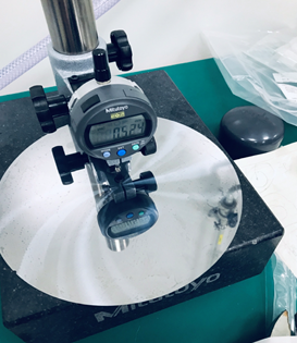
It is used for thinning 8-inch and smaller wafers (including SOI, silicon, glass, copper sheets and other semiconductor materials), with a thickness accuracy within 2 μm. The equipment facilitates the subsequent packaging process.
Process / Testing Capabilities
It is applicable to the thinning of 8-inch and smaller wafers, including SOI, silicon, glass, copper sheets and other semiconductor materials. The thickness accuracy can be controlled within 2 μm, and the equipment provides convenience for subsequent packaging processes.
Technical Specifications
Address: 800 Dongchuan Road, Minhang District, Shanghai 200240, China
Tel: +86 21 3420 7734
Email: aemd@sjtu.edu.cn


