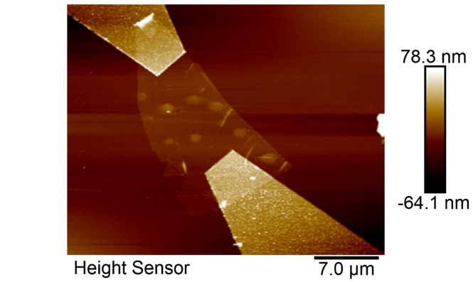
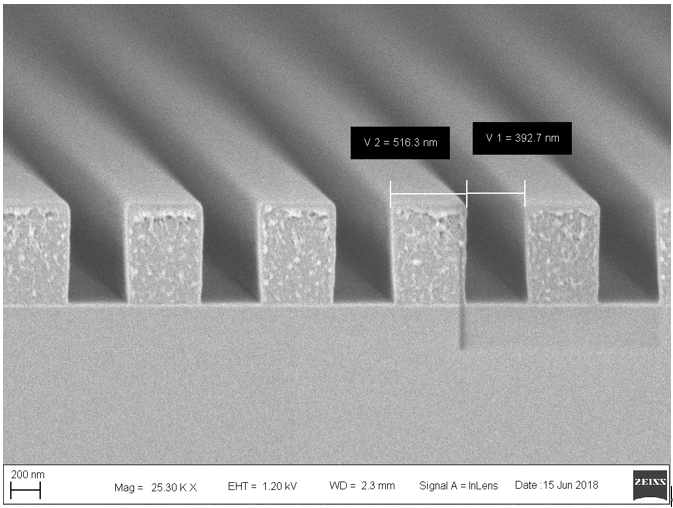
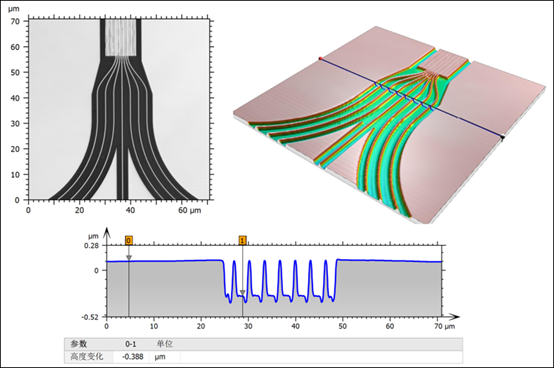
EN
EN
CN
Contact Us
Careers
Direction
Login
About Us
Facilities
Process Capabilities
Services & Products
User Guide
Home
About Us
返回
About Us
Platform Overview
Platform History
Staff
Staff Zone
Careers
Direction
Facilities
返回
Facilities
Micro-/Nano Fabrication
Packaging Processes
Characterisation & Testing
Process Capabilities
返回
Process Capabilities
Fabrication Processes
Testing & Characterisation
Process Integration
Services & Products
返回
Services & Products
Service Models
Supported Fields
Industry Engagement
Semi-Finishied-Products
Contract Manufacturing Services
User Guide
返回
User Guide
How to Become a User
EHS
Downloads
FAQs
Login
网站底部链接
返回
网站底部链接
服务平台链接
Login
Home
>
Process Capabilities
>
Testing & Characterisation
>
Surface Morphology Measurement
Testing & Characterisation
Surface Morphology Measurement
Film Thickness Measurement
Thin Film Property Characterisation
Electrical/Optical Characterisation of Devices & Chips
Surface Morphology Measurement
Film Thickness Measurement
Thin Film Property Characterisation
Electrical/Optical Characterisation of Devices & Chips
表面形貌量测
AFM观察测量2D材料表面形貌:
SEM
观察测量光栅侧壁结构:
激光共聚焦显微镜观察测量三维光栅波导结构:
×