Scroll down
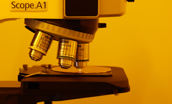
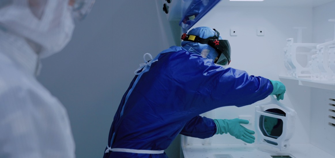
The platform supports micro- and nano-fabrication processes for silicon, glass, III–V compound semiconductors, and organic materials. Core processes include photolithography (electron-beam lithography, KrF deep ultraviolet lithography, and double-sided UV lithography), wet and dry etching, thin-film deposition, packaging, electroplating, and oxidation and diffusion. Equipped with a full chain of processing tools, the platform enables integrated fabrication and testing capabilities for devices and patterns ranging from 10 nm to the micron scale.
A wide range of characterization and testing equipment enables in-line and off-line process monitoring and characterization, as well as electrical and optoelectronic performance evaluation.
Possesses integrated process capabilities for various types of micro- and nano-devices, providing users with customized fabrication and R&D services.
为了营造和谐向上的团队文化氛围,增强平台教职员工归属感和幸福感,AEMD平台
在基片上沉积各种材料的薄膜是微纳加工的重要手段之一,主要方法有化学气相沉积、蒸发、溅射等。
干法刻蚀是用等离子体化学活性较强的性质进行薄膜刻蚀的技术。
电镀是利用电解原理使金属或合金沉积在基底表面,以形成均匀、致密、结合力良好的金属层的过程。
IC制程中需要一些有机试剂和无机试剂参与完成,另外,制作过程总是在人的参与下在净化室中进行,这样就不可避免各种环境对硅片污染的情况发生。