| Model: | DAD3650 |
|---|---|
| Function: | It adopts blade physical dicing.Applicable materials: silicon wafer, SOI, glass, quartz, sapphire, silicon carbide, ceramic and other semiconductor materials. |
| Engineer: | Ms.Liu / +86-21-34207734-8016 / liuxinyuan@1 |
| Location: | West Area Packaging Zone I |
| Equipment ID: | WT1DDAD01 |

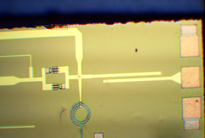
The DAD3650 equipment is applicable for dicing of semiconductor materials such as silicon wafers, SOI wafers, glass, quartz, sapphire, silicon carbide, ceramics and PCB substrates.
Process / Testing Capabilities
Suitable for dicing wafers with a size of 8 inches and below (including irregular-shaped wafers). The applicable wafer thickness ranges from 100 μm to 2500 μm. Processable wafer materials include silicon wafers, SOI, glass, quartz, sapphire, silicon carbide, ceramics, PCB circuits and other semiconductor materials.
Chipping for blank silicon wafer dicing: less than 10 μm; chipping for silicon oxide ceramic wafers and glass: less than 50 μm.
Technical Specifications
2.5mm
Address: 800 Dongchuan Road, Minhang District, Shanghai 200240, China
Tel: +86 21 3420 7734
Email: aemd@sjtu.edu.cn


