| Model: | EVG510 |
|---|---|
| Function: | 1. Achieve tight bonding of two or more wafers to realize high-density interconnection among multiple wafers, which is widely applied especially in 3D IC packaging. 2. Support a variety of wafer bonding processes, including anodic bonding, eutectic bonding, thermocompression bonding and others. 3. Compatible with the EVG-610 lithography machine to realize wafer alignment and positioning functions. 4. Be compatible with pre-processes such as plasma cleaning and wet cleaning for wafer surface treatment in the early stage. |
| Engineer: | Zhang / +86-21-34206126-6029 / captianzhangdi@1 |
| Location: | East Area – Lithography II (Canon) |
| Equipment ID: | ELT2WBS01 |

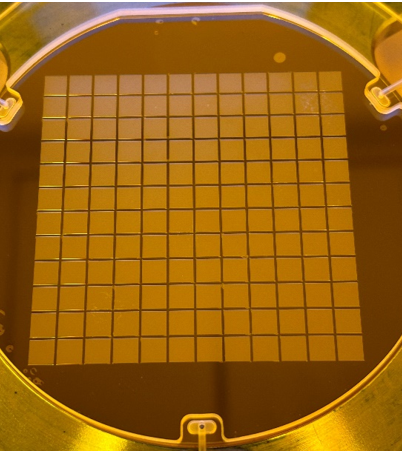
A wafer bonding equipment achieves high-precision wafer bonding through thermal, pressure and vacuum technologies.
Optical Alignment: The high-precision alignment system uses microscopes and alignment marks to register wafers, achieving sub-micron level accuracy.
Pressure Control: Uniform pressure is applied via pneumatic or mechanical loading to ensure intimate wafer contact and eliminate voids.
Thermal Treatment: The heating stage provides controllable temperature to activate bonding materials or promote chemical reaction curing.
Vacuum Environment: The vacuum chamber reduces bubble formation and optimizes the quality of the bonding interface.
Automated Process: It supports full-process automatic control of heating, pressurization and cooling to guarantee excellent repeatability and reliability.
The EVG510 is suitable for bonding of various materials such as silicon-to-silicon, silicon-to-glass and a wide range of metals, and is widely applied in MEMS device fabrication and wafer-level packaging.
Process / Testing Capabilities
Technical Specifications
Address: 800 Dongchuan Road, Minhang District, Shanghai 200240, China
Tel: +86 21 3420 7734
Email: aemd@sjtu.edu.cn


