High-precision Optoelectronic Chip Coupling System
FLIP-CHIP BONDER
Operating
Model: ACCμRA OPTO
Function: High-precision flip-chip interconnection and coupling process for optoelectronic chips, laser chips and other related chips. It supports cold pressure welding, reflow soldering, in-situ reflow, flux-free eutectic bonding, thermocompression bonding and other processes for various types of chips.
Engineer: Ms.Liu / +86-21-34206126-6027 / liudanqh@1
Location: East Area, Packaging Zone II
Equipment ID: EPK2EOC01
  • Basic Equipment Information
  • Operating Principle
  • Typical Application Case
Main Application

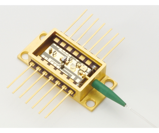
The high-precision optoelectronic chip coupling system is specially designed for high-precision low-pressure bonding and reflow soldering processes, and is applied to high-precision flip-chip interconnection and coupling of optoelectronic chips, laser chips and other similar chips.


Process / Testing Capabilities

  • The equipment supports cold pressure welding, reflow soldering, in-situ reflow, flux-free eutectic bonding, thermocompression bonding and other processes for various types of chips.
  • It is equipped with flip-chip bonding and face-up bonding functions, enabling chip-to-chip and chip-to-wafer bonding modes.
  • Bonding media including gold, gold-tin, tin, tin-silver, indium and copper are supported; independent temperature control of the upper and lower chips can be realized in pressure welding processes.


Technical Specifications

  • Interconnection accuracy: ±0.5 μm;
  • Bonding pressure: 0.2~10N;
  • Temperature control range: Room temperature to 400 ℃ (bond arm); Room temperature to 400 ℃ (stage); resolution: 1 ℃;
  • Chip size: 0.25×0.25 mm – 22×22 mm (bond arm), 2×2 mm – 50×50 mm (stage)
The high-precision optoelectronic chip coupling system adopts a vision alignment system with a fixed beam splitter, which realizes accurate visual alignment between chips and substrates to achieve high-precision bonding and soldering.
Optoelectronic Device Assembly(Images sourced from official equipment website promotional materials).

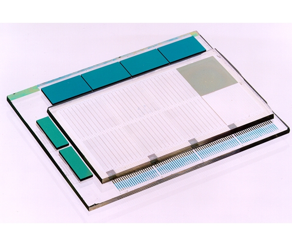
Multi-Chip Module(Image sourced from the official promotional picture on the equipment website)

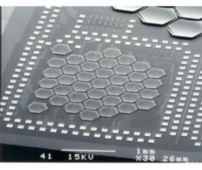
MEMS Packaging (Images sourced from official promotional pictures on the equipment website)

Both the front and back surfaces of the sample shall be kept clean, especially the back surface shall be free from contamination and particulate matter.
The list below shows FAQs (click a question to view the answer). If your question is not listed, you can leave a message using the link.
FAQs
  • 01
    为什么不同芯片需要单独的芯片吸盘(TOOL)?

    一般建议芯片吸盘的真空区域占芯片总面积的50%及以上,避免因为真空吸附引起芯片翘曲从而影响最终键合效果。

Message Inquiry
If your question is not listed above, please email us at aemd@sjtu.edu.cn or click the button below to submit an inquiry.
Note: "@1" represents "@sjtu.edu.cn"
×