| Model: | 150 |
|---|---|
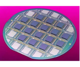
| Function: | Supports cold pressing, thermocompression reflow and eutectic processes for various types of chips. The equipment is capable of flip-chip bonding and face-up bonding, enabling bonding modes such as chip-to-chip and chip-to-wafer. |
| Engineer: | Liu / +86-21-34206126-6027 / liudanqh@1 |
| Location: | East Area – Packaging II |
| Equipment ID: | EPK2FCB01 |

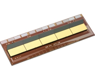
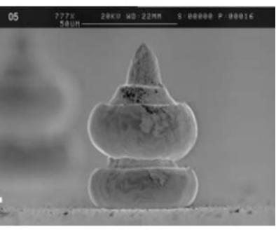
The high-force chip bonder features precise parallelism adjustment capability for chips, high bonding pressure and superior bonding accuracy, enabling its extensive applications in the assembly of optoelectronic and photonic devices, focal plane devices, 3D integration and other related fields.
Process / Testing Capabilities
Technical Specifications
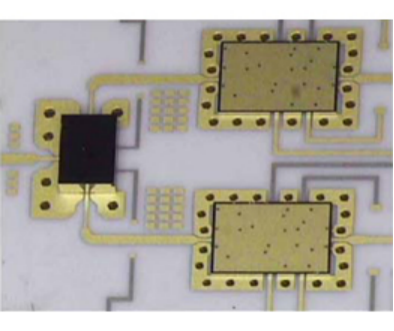
Radio Frequency Device(Image sourced from promotional materials on the equipment official website)
Address: 800 Dongchuan Road, Minhang District, Shanghai 200240, China
Tel: +86 21 3420 7734
Email: aemd@sjtu.edu.cn


