| Model: | AM222-TPPP |
|---|---|
| Function: | Capable of depositing high-quality piezoelectric AlN, AlScN thin films and Mo metal, as well as achieving ultra-smooth planarization treatment of thin films. |
| Engineer: | Wu / +86-21- 34206126-6028 / lynn_wu@1 |
| Location: | East Area – Thin Film IV |
| Equipment ID: | EFM4HVM01 |

This system is a highly integrated multi-chamber magnetron sputtering equipment, specially designed for the research and fabrication of high-performance microelectronic and acoustic devices, including BAW filters, SAW devices, MEMS sensors and other related components.
It is equipped with four process chambers: an AlN thin film sputtering chamber, an AlScN thin film sputtering chamber, a molybdenum (Mo) metal sputtering chamber, and an ion beam chamber for fine planarization and trimming of thin films.
The core application is the fabrication of piezoelectric thin-film devices with aluminum nitride (AlN) and scandium-doped aluminum nitride (AlScN) as the key functional materials.Thin films deposited by sputtering often exhibit insufficient surface flatness, and surface roughness severely degrades the performance of high-frequency devices, such as increased power loss. The ion beam planarization chamber is adopted to achieve ultra-smooth surface finishing of deposited films.
Process/Testing Capability
It enables the deposition of piezoelectric AlN, AlScN thin films and molybdenum (Mo) metal, as well as ion beam fine planarization and trimming of thin films.The process ensures a highly ordered crystalline structure of films. The preferred crystallographic orientation of AlN and AlScN is the (002) plane, while that of Mo is the (110) plane.The fabricated films feature low crystal defects and residual stress, making them highly suitable for the fabrication of piezoelectric surface acoustic wave devices such as SAW and F‑bar components.
Technical Specifications
1.Only intact wafers are acceptable as substrates, with available sizes of 4-inch, 6-inch and 8-inch.
2.Chamber vacuum level: 5×10⁻⁷ Torr.
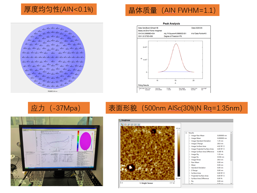
3.Thickness uniformity (1 sigma/mean) of planarized 8-inch wafers:
a) 1 μm AlN: uniformity < 0.1%;
b) 500 nm AlSc(30%)N: uniformity < 0.1%;
c) 300 nm Mo: uniformity < 0.7%.
4.The thin films possess a highly ordered crystalline structure. AlN and AlScN exhibit a preferred (002) crystallographic orientation, while Mo shows a preferred (110) crystallographic orientation.
5.Crystalline quality after planarization:
a) XRD rocking curve FWHM of AlN < 1.5°;
b) XRD rocking curve FWHM of AlSc(30%)N < 1.7°;
c) XRD rocking curve FWHM of Mo < 2°.
Magnetron sputtering utilizes the combined effects of magnetic and electric fields to bombard target materials (e.g., AlSc alloys) within plasma. This process ejects target atoms or molecules, which then deposit onto substrates to form thin films.
Working Principle of Trimming
1. The wafer travels at a constant speed, while the power is adjusted according to thickness or frequency uniformity mapping.
2. The ion source power is varied to control the amount of material removed from the wafer.
3. Benefiting from constant wafer motion, the Advanced Trimming System (AMS) adopts a simple and robust wafer scanning mechanism.
4. The minimum etch rate can reach zero. No additional material deposition is required, eliminating device performance degradation. This is critical for frequency trimming of surface acoustic wave (SAW) devices.
1.To ensure optimal performance, prime-grade silicon substrates are recommended (available for paid collection on the platform).
2.For AlN, AlScN and Mo deposition, N-type and low-resistivity Si substrates (< 5 Ω·cm) are prohibited, as they may compromise deposition quality.
3.This tool is a large-scale integrated multi-chamber system. For superior performance in terms of thickness uniformity, crystalline orientation and other indicators, the full-process workflow — including substrate pretreatment and planarization — is highly recommended.
4.If only standalone deposition is required, independent deposition recipes are listed separately. Note that standalone deposition is unavailable for 30% AlScN, while offered for AlN and Mo. Such single-deposition jobs may require batching with other orders, which may lead to longer lead times. Your understanding is appreciated.
5.No cracked or broken wafers are permitted in any chamber (deposition and planarization). Currently supported wafer sizes: 8-inch, 6-inch and 4-inch.
6.Charging standards are unified for all chambers (deposition and planarization), billed per wafer per run regardless of wafer size.
7.The maximum Total Thickness Variation (TTV, Max-Min) of the planarization chamber is 30 nm. Samples exceeding this range require repeated planarization with additional charges.
8.The current standard Sc doping concentration provided by the platform is 30%. Please contact the engineer if 20% Sc doping is required.
9.Bulk orders of more than 10 pieces are eligible for discounted rates upon consultation with the engineer.
Address: 800 Dongchuan Road, Minhang District, Shanghai 200240, China
Tel: +86 21 3420 7734
Email: aemd@sjtu.edu.cn


