| Model: | EBPG 5200 |
|---|---|
| Function: | Direct-write lithography for nanoscale structures on substrates up to 8 inches |
| Engineer: | Xu / +86-21-34206126-6018 / xu.jian@1 |
| Location: | West Area – Lithography I |
| Equipment ID: | WPHVEBL01 |

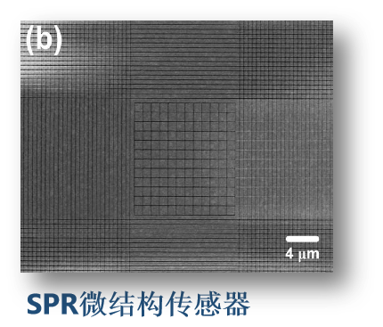
Exposure of nanoscale patterns for micro/nano device fabrication. Suitable for various nanostructures and devices, photomasks, nanoimprint templates, etc.
The principle of electron beam lithography is based on the interaction between electrons and matter. Electromagnetic lenses at various stages deflect and focus the electron beam emitted from the electron source. A beam blanker controls the on/off switching of the beam, enabling pattern scanning onto the wafer.
LNO modulator
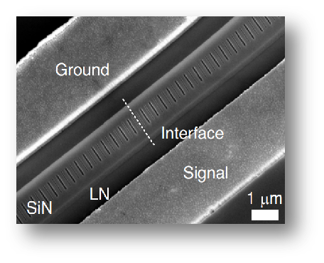
Sub-100 nm 2D grating
Material Type: Standard semiconductor silicon wafers suitable for vacuum environment; non-magnetic materials:
Si, GaAs, GaN, GaP, metal-coated glass
Substrate Dimensions: 2", 3", 4", Φ125 mm, Φ150 mm, Φ200 mm
Thickness: Max. 0.675 mm
Non-standard substrates must be ≥10 mm × 10 mm
Photomask (chrome mask) dimensions: 3", 4", 5", 6", 7"
Thickness: Max. 0.09" @ 5" mask
Max. 0.25" @ 6" mask
Direct-write pattern area: Up to ~210 mm × 210 mm
Substrate flatness:
Max. ±30 μm peak-to-peak (without alignment marks)
Max. ±50 μm peak-to-peak (with alignment marks)
(For non-standard substrates with special thickness, three additional samples of the same thickness are required for height reference.)
PMMA, CSAR62 (HSQ, ZEP can be provided by user)
Check the reservation notice on the platform homepage.
Address: 800 Dongchuan Road, Minhang District, Shanghai 200240, China
Tel: +86 21 3420 7734
Email: aemd@sjtu.edu.cn


