ICP-CVD
Inductively Coupled Plasma Chemical Vapor Deposition System
Operating
Model: PlasmaPro 100 ICPCVD180
Function: Sample size: up to 6 inches; low-temperature deposition of silicon dioxide and silicon nitride thin films.
Engineer: Mr. Fu / +86-21- 34206126-6010
Location: Thin Film Zone II, West Area
Equipment ID: WF2PCVD01
  • Basic Equipment Information
  • Operating Principle
  • Typical Application Case
Main Application

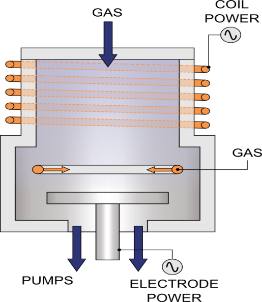
Supports low-temperature deposition of silicon dioxide and silicon nitride thin films to meet the requirements of lift-off processes. It can also deposit high-quality silicon nitride, silicon oxide, silicon oxynitride and amorphous silicon thin films at high temperature.


Process/Testing Capability

It meets the requirements for depositing silicon dioxide films with a thickness below 10 μm and silicon nitride films below 5 μm. It is capable of preparing ultra-low stress dielectric films with stress less than 10 MPa.


Technical Specifications

  1. The maximum sample size is 6 inches.
  2. Deposition rate of silicon dioxide: adjustable from 20 nm/min to 100 nm/min.
  3. Deposition rate of silicon nitride: adjustable from 5 nm/min to 20 nm/min.
  4. Refractive index of silicon dioxide: adjustable within 1.45–1.49.
  5. Refractive index of silicon nitride: adjustable within 1.85–2.10.
High-purity nitrogen or nitrous oxide enters the reaction chamber independently from the top and is excited by an alternating electric field. Silane is injected into the chamber near the sample surface and reacts with nitrogen ions to form silicon nitride thin films. Backside cooling helium gas is introduced through air holes on the substrate stage to dissipate heat and control the temperature of the substrate. The substrate is tightly pressed by a quartz compression ring to prevent helium leakage into the chamber and avoid adverse impacts on the process.Since the plasma is kept away from the substrate, surface damage of the deposited thin film is greatly reduced. With this indirect ICP-PECVD configuration, although the plasma density is high, the ion energy on the substrate remains low. The resulting silicon nitride thin films feature superior surface passivation performance and excellent thermal stability.


Low-temperature preparation of ultra-thick silicon dioxide films.


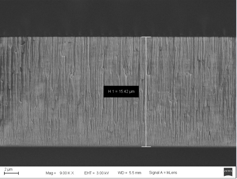
An ultra-thick silicon dioxide film with a thickness of 15.4 μm is prepared at a deposition temperature of 65 ℃. The film presents no cracking, deformation or pores, and possesses preferred crystal orientation.

Sample size no more than 6 inches, enabling low-temperature deposition of silicon dioxide and silicon nitride thin films.
Involving special gas and ionizing radiation, please strictly follow operational specifications.
The list below shows FAQs (click a question to view the answer). If your question is not listed, you can leave a message using the link.
FAQs
  • 01
    在实验过程遇到设备报警实验中断怎么办?

    及时联系工程师查找记录,确定已完成的的时间,争取让实验正常完成

Message Inquiry
If your question is not listed above, please email us at aemd@sjtu.edu.cn or click the button below to submit an inquiry.
Note: "@1" represents "@sjtu.edu.cn"
×