Ultra High Vacuum Sputtering System
Ultra-High Vacuum Sputtering System
Operating
Model: MPS-3000-HC5
Function: 1.Sputtering deposition of various metal thin films; 2.Sputtering of magnetic materials requires prior confirmation from the platform management team.
Engineer: Mr. Mao / +86-21- 34206126-6009 / maohaiping@1
Location: West Zone, Thin Film Area IB
Equipment ID: EMCUUVS01
  • Basic Equipment Information
  • Operating Principle
  • Typical Application Case
Main Application

Ultra-high vacuum sputtering system is used to deposit single-layer or multilayer nanoscale thin films such as Pd, Ti, Zr, Ta and Al, with typical thicknesses below 50 nm.


Process/Testing Capability

  • Film thickness: several nm ~ 100 nm; Sputtering rate: 2–4 nm/min
  • Film uniformity and repeatability: For 3-inch substrates, the uniformity is better than ±2%, and the repeatability is better than ±2%.
  • Target size: 2 inches; 4 target positions; equipped with 1 RF power supply and 2 DC power supplies.


Technical Specifications

  • Ultimate vacuum: better than 1×10⁻⁶ Pa
  • Substrate size: 3-inch wafers and diced pieces
  • DC power: 0–200 W; RF power: 0–250 W
  • Conventional process: DC power 5–100 W; base vacuum
  • Base pressure: 0×10−5 Pa; working pressure: 0.107 Pa; Ar gas flow: 17.8 sccm
The principle of sputter coating relies on plasma generated by abnormal glow discharge in a rarefied gas. Under the action of an electric field, charged particles bombard the surface of the cathode target, ejecting molecules, atoms, ions, and electrons from the target. These sputtered particles carry kinetic energy and travel in a directional manner toward the substrate, eventually forming a uniform thin film on its surface. An ultra-high vacuum working environment reduces the evaporation temperature of metallic and other materials, while effectively improving the sputtering rate.
1.After 1800 seconds of sputtering, the surface roughness reaches 0.90 nm.


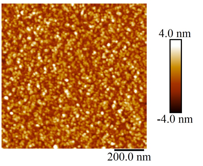
2.After sputtering for 5200 seconds, the surface roughness is 1.60 nm.


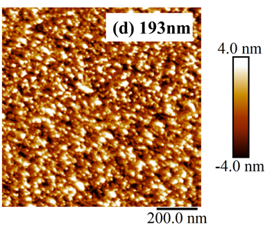
Conclusion: The sputtered material is zirconium oxynitride thin film. As the sputtering time increases, the film thickness grows gradually, and fine grains aggregate into larger ones, which leads to an increase in surface roughness. In addition, sputtered particles deposit onto the substrate surface from multiple directions and may induce asymmetric growth. With prolonged sputtering duration, such asymmetric crystal growth further causes a continuous rise in the surface roughness of the thin film.

 
  1. Users must register as platform members and submit a processing reservation application. Processing and experiments are permitted only after official approval.
  2. Prohibited samples:

Samples with high humidity, and photoresist specimens susceptible to thermal denaturation at high temperature.

  1. Permitted samples:

Samples with clean surfaces and a size of no more than 3 inches.

Film deposition on photoresist-coated substrates is prohibited.

Reactive sputtering under an oxygen atmosphere is not allowed.

Sample specification: 3-inch size. Deposition on photoresist-coated substrates and reactive sputtering in an oxygen atmosphere are prohibited. Charging is calculated with a minimum unit of 0.5 hours. Refer to the operation manual for detailed procedures.
The list below shows FAQs (click a question to view the answer). If your question is not listed, you can leave a message using the link.
FAQs
  • 01
    遇到突发事件如断水,断电,断气

    按请立即按EMO 按钮.

Message Inquiry
If your question is not listed above, please email us at aemd@sjtu.edu.cn or click the button below to submit an inquiry.
Note: "@1" represents "@sjtu.edu.cn"
×