Metal Thin Film Etcher
ICP Reactive Ion Etching System- For Metal Films
Operating
Model: SI500
Function: 1. Etching of metal films such as Al, Ni, Cr and Ti; 2. Etching of organic thin films; 3. Etching of other thin film materials.
Engineer: Mr.Zhang / +86-21- 34206126-6020 / dzlzhangyan@1
Location: East Area, Thin Film IV Zone
Equipment ID: WF2SRIE01
  • Basic Equipment Information
  • Operating Principle
  • Typical Application Case
Main Application

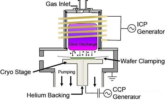
This equipment is mainly used for the micro-nano structure etching of metals, metal oxide thin films and various organic materials.


Process / Testing Capabilities

It enables anisotropic etching of metals including Al, Cr and Ni, various organic materials such as BCB, PR, PI and PDMS, as well as substances like lithium niobate and lithium carbonate.


Technical Specifications

This system is engineered for 8-inch wafers and backward compatible with 6-inch, 5-inch, 4-inch, 3-inch substrates, as well as various fragmented samples for etching processes. It is equipped with multiple process gases, including Cl2, BCl3, HBr, SF6, CF4, CHF3, Ar, N2 and O2.

ICP-RIE (Inductively Coupled Plasma-Reactive Ion Etching) is an advanced process technology that integrates ICP and reactive ion etching (RIE). It is designed to achieve high etching rates, excellent etching selectivity and low-damage etching. Since the plasma can be sustained under low-pressure conditions, this technology also delivers superior profile control.First, the ICP-RIE system introduces designated etching gases. Radio frequency power (typically 13.56 MHz) is supplied to a conductive coil mounted on the top of the plasma reaction chamber, which is isolated from the internal gas atmosphere of the chamber. When RF power is applied to the coil, an oscillating electromagnetic field is generated around the conductor. The energy of this oscillating electromagnetic field is transferred to the gas inside the reaction chamber through inductive coupling. This excites electrons in gas molecules and strips them from atoms, generating free electrons and positive ions. These free electrons continuously gain energy in the electromagnetic field and collide with additional gas molecules, triggering further electron dissociation and eventually forming high-density plasma.

The figure shows the etched structure of LNOI thin film.
This equipment is mainly used for etching samples such as metal thin films and various organic thin film materials. Highly contaminated samples (e.g., lead-containing materials, SiC, etc.) and samples larger than 8 inches are not accepted.
The list below shows FAQs (click a question to view the answer). If your question is not listed, you can leave a message using the link.
FAQs
  • 01
    设备接受哪些种类的掩膜材料?

    该设备可接受的掩膜材料有普通光刻胶,SiO2或SiNx,a-Si等各种硬掩模材料。

Message Inquiry
If your question is not listed above, please email us at aemd@sjtu.edu.cn or click the button below to submit an inquiry.
Note: "@1" represents "@sjtu.edu.cn"
×