| Model: | developer |
|---|---|
| Function: | Spray-type development for substrates up to 6 inches. |
| Engineer: | Wang / +86-21- 34206126-6005 / fdwang@1 |
| Location: | West Area – Lithography I |
| Equipment ID: | WPHLEDC01 |

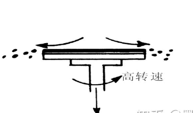
After exposure, wafers are processed in the developer using a developing solution to remove selected regions of photoresist.
Spray-type development for substrates up to 6 inches.
Development is the process of placing exposed wafers into the developer and applying a developing solution to remove either exposed or unexposed photoresist, depending on the process type.
Supports standard wafers from 2” to 6”. Supports fragments larger than 10 mm × 10 mm.
Supports standard wafers from 2” to 6”. Supports fragments larger than 10 mm × 10 mm.
Clean the chuck surface and the backside of the wafer promptly
Address: 800 Dongchuan Road, Minhang District, Shanghai 200240, China
Tel: +86 21 3420 7734
Email: aemd@sjtu.edu.cn


