| Model: | Spin-coater |
|---|---|
| Function: | 1.Photoresist spin coating ; 2.Spin coating of flexible substrate precursor materials. |
| Engineer: | Wang,Zhang / +86-21- 34206126-6005/6029 / fdwang@1/captianzhangdi@1 |
| Location: | East Area – Lithography IIIA, West Area – Lithography I |
| Equipment ID: | ELT3SPC01、WPHSCOT02、WPHSCOT01、EPHKCOT01 |

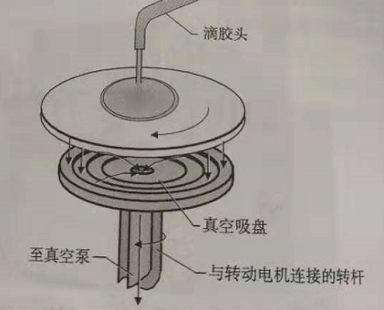
Uniformly coat photoresist onto substrates using the spin coating method.
Spin coating of photoresist for wafers up to 6 inches.
The spin coater operates by uniformly distributing photoresist onto the substrate through high-speed rotation.
Semiconductor standard silicon wafers or glass substrates.
Fragments smaller than 1" (minimum 10 mm × 10 mm), standard wafers: 2", 3", 4", 6".
Check the equipment status before use and ensure proper sample placement. After spin coating, thoroughly clean the chamber immediately. Cleaning may also be performed after each session if it does not interfere with other scheduled users. Typically, use lint-free wipes soaked in acetone to remove photoresist residues.
Clean the chuck surface and the backside of the wafer promptly
Address: 800 Dongchuan Road, Minhang District, Shanghai 200240, China
Tel: +86 21 3420 7734
Email: aemd@sjtu.edu.cn


