| Model: | MA/BA6 |
|---|---|
| Function: | 1.Micro-nano structure and device pattern lithography; 2.Double-sided alignment lithography. |
| Engineer: | Wang / +86-21-34206126-6005 / fdwang@1 |
| Location: | West Area – Lithography I |
| Equipment ID: | WPHSMAL01 |

Process micron-scale structural patterns in micro-nano devices. Transfer the designed circuit patterns onto photoresist, and then transform them into actual circuit patterns through processes such as etching.
Exposure of micron-scale structural patterns in micro-nano device processing, resolution: 0.8 μm, front-side alignment accuracy: ±0.5 μm, back-side alignment accuracy: ±1 μm, supports wafers of 6, 4, 3 inches or below and fragmented wafers.
Resolution: 0.8μm, front registration accuracy: ±0.5μm, back registration accuracy: ±1μm, supports wafers and fragments below 6, 4, and 3 inches.
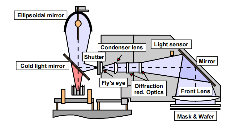
Its working principle is to expose the pattern on the photomask onto the spin-coated photosensitive material by controlling the light intensity and time, and then transfer the pattern to the substrate after development.
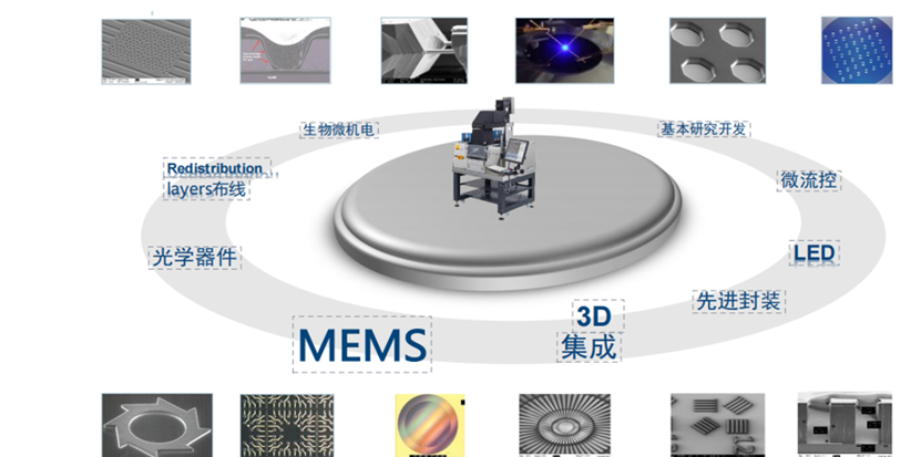
MEMS process processing, advanced packaging, microfluidics, optical device manufacturing, RDL wiring, and basic research and development, etc.
1. Supports wafers and fragments below 6 inches. Both the front and back sides of the samples must remain flat, clean and tidy. The complete process includes photoresist spin-coating, hot plate baking, development and observation under an ordinary microscope.
2. Costs for special photoresists are charged separately.
3. Thick photoresist processes are charged separately.
4. Substrates and photomasks are not included.
5. Photomask size requirements: compatible with 4", 5" and 7" photomasks.
1. Supports wafers and fragments smaller than 6 inches. Both the front and back sides of the samples must remain flat, clean and tidy. The complete process includes photoresist spin-coating, hot baking, development and observation under an ordinary microscope.
2. Fees for special photoresists are charged separately.
3. Thick photoresist processes are charged separately.
4. Substrates and photomasks are not included.
5. Photomask size requirements: support for 4", 5" and 7" photomasks.
6.Independent machine operation is only allowed after obtaining machine operation qualification certification.
Please clean the back of the wafer in time.
Address: 800 Dongchuan Road, Minhang District, Shanghai 200240, China
Tel: +86 21 3420 7734
Email: aemd@sjtu.edu.cn


