| Model: | Candela 8400 |
|---|---|
| Function: | It is used for inspection and analysis of wafer surface defects. It rapidly classifies defects (including particles, scratches, pits, watermarks, and residue marks), counts the number of each defect type, and measures the corresponding defect sizes. Finally, it generates a defect distribution map of the entire surface and a detailed inspection report. Based on predefined defect criteria, the system can also determine whether the inspected sample passes or fails. |
| Engineer: | Qu / +86-21- 34207734-8003 / minni.qu@1 |
| Location: | East Area – Thin Film IV |
| Equipment ID: | EFM4OSA01 |

This equipment is a semi-automated wafer surface defect inspection and analysis system designed for the semiconductor and compound semiconductor industries.
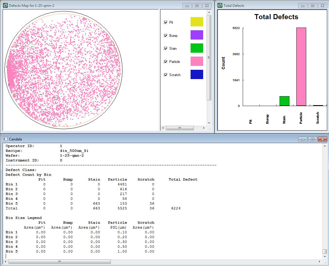
It scans the entire surface of the sample using a laser beam. Based on signals collected by detectors in four channels—scattered light, reflected light, phase shift, and Z channel—it rapidly classifies defects (including particles, scratches, pits, watermarks, and residue marks), counts each defect type, and measures the corresponding defect sizes. Finally, it generates a full-surface defect distribution map and a comprehensive inspection report.
Process/Testing Capabilities
It is used to monitor and analyze various defects across different process steps, investigate their root causes, and develop methods for eliminating or preventing defect formation. It can effectively improve device yield affected by surface defects in a targeted manner. The system also provides important support for process optimization, environmental improvement, device quality monitoring, yield enhancement, and improved manufacturing efficiency.
Technical Specifications
● 405 nm wavelength laser, spot diameter ≤ 15 µm
● Maximum sample size: 8-inch wafer
● Defect sensitivity (minimum detectable size):
Particles: diameter ≥ 83 nm (PSL on Si)
Scratches: length ≥ 100 µm, width ≥ 0.1 µm, depth ≥ 5 nm
Pits: diameter ≥ 20 µm, depth ≥ 5 nm
Contamination (liquid residue): diameter ≥ 20 µm, thickness ≥ 1 nm
The intensity, direction, and phase of the scattered light are closely correlated with defect characteristics such as size, shape, and composition.
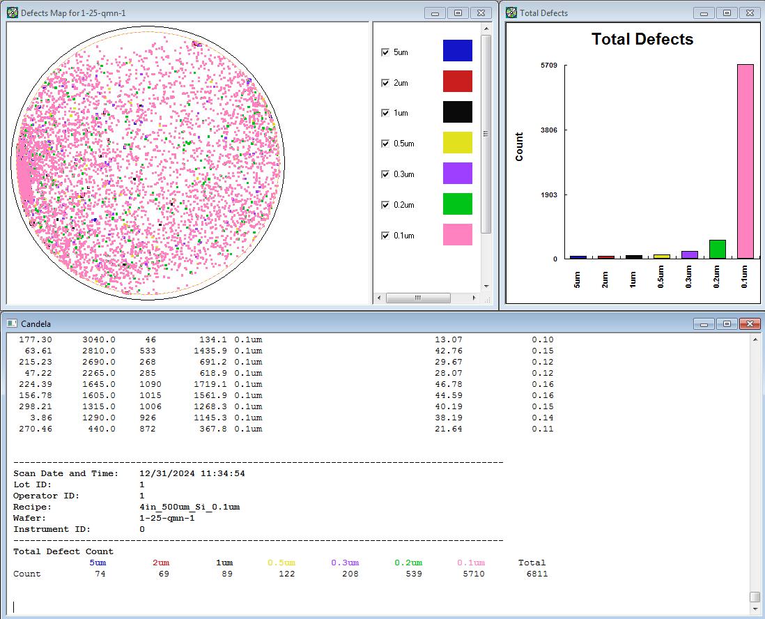
Example of defect detection results for different defect types on a 4-inch silicon wafer surface.
Address: 800 Dongchuan Road, Minhang District, Shanghai 200240, China
Tel: +86 21 3420 7734
Email: aemd@sjtu.edu.cn


