| Model: | GSE200plus |
|---|---|
| Function: | 1.Etching of dielectric thin films such as silicon dioxide (SiO₂), silicon nitride (Si₃N₄), and silicon oxynitride (SiON); 2.Etching of silicon carbide (SiC) thin films; 3.Quartz etching. |
| Engineer: | Liu / +86-21- 34206126-6013 / minliu@1 |
| Location: | West Area – Thin Film II |
| Equipment ID: | WF2NRIE02 |

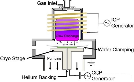
This system is primarily used for etching:
Dielectric thin films such as SiO₂, Si₃N₄, and SiON;SiC thin films;Quartz substrates
Process / Testing Capabilities
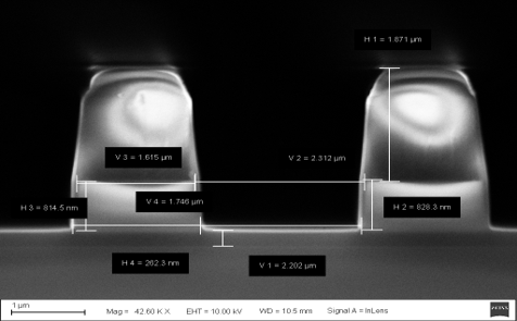
Etch rate for SiO₂ or Si₃N₄: >400 nm/min. Selectivity to photoresist: ~2:1. Sidewall angle: >85°. Within-wafer uniformity: <5%
Technical Specifications
Designed for 6-inch wafers. ICP power: up to 1500 W. Bias power: up to 500 W. Supported etching gases: CHF₃, SF₆, CF₄, Ar, O₂, N₂
During operation, etching gases are introduced into the chamber. A radio frequency (RF) power source (typically 13.56 MHz) is applied to a coil positioned above the chamber, generating an oscillating electromagnetic field. Through inductive coupling, energy is transferred to the gas, ionizing it and forming a high-density plasma consisting of free electrons and ions.
These energetic species interact with the substrate surface, enabling controlled chemical and physical etching under low-pressure conditions, providing excellent anisotropy and profile control.
Samples larger than 6 inches are not accepted.
Contaminated samples are not permitted.
Address: 800 Dongchuan Road, Minhang District, Shanghai 200240, China
Tel: +86 21 3420 7734
Email: aemd@sjtu.edu.cn


