Ion Beam Sputtering System, IBD
Ion Beam Sputtering System
Operating
Model: LDJ2B-F100-100
Function: Deposit various metallic thin films;Deposition of magnetic materials requires prior consultation and confirmation with the platform.
Engineer: Mr. Mao / +86-21- 34206126-6009 / maohaiping@1
Location: Thin Film Zone IA, West Area
Equipment ID: EMCAIBD01
  • Basic Equipment Information
  • Operating Principle
  • Typical Application Case
Main Application

Dual Ion Beam Sputtering System is applied for the sputtering deposition of single-layer and multilayer films including Ti, Cr, Ni, Cu, Au and other materials. It supports ion beam cleaning (IBC) and ion beam sputtering deposition (IBSD).


Process/Testing Capability

Coating uniformity and repeatability: The uniformity on 4-inch substrates is better than ±5%, with repeatability superior to ±5%.Equipped with two 4-inch target positions and two sets of ion sources.Supports Ion Beam Cleaning (IBC) mode and Ion Beam Sputtering Deposition (IBSD) mode.


Technical Specifications

  • Ultimate vacuum: 2×10⁻⁴ ;
  • PaSubstrate size: 4-inch substrates with a thickness less than 4 mm are supported;
  • Deposited film uniformity: ±5%;
  • film thickness measurement resolution: 0.2 nm;
  • film growth rate measurement resolution: 0.2 nm/s
Ion Beam Sputtering (IBS), also referred to as Ion Beam Deposition (IBD), is a thin-film deposition process. It utilizes an ion source to sputter target materials (metals or dielectrics) and deposit them onto substrates, forming metallic or dielectric films. Featuring monoenergetic ions with uniform energy and high collimation, IBS enables precise thickness control and the deposition of highly dense, high-quality thin films compared with other Physical Vapor Deposition (PVD) technologies.
Comparison of AFM imaging on surface roughness of double-sided polished quartz substrates after sputtering gold films with different thicknesses


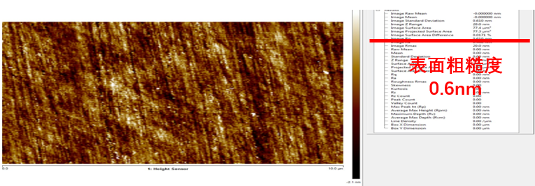
Figure 1 AFM image of the quartz surface roughness before sputtering


Figure 2 Surface roughness measurement after sputtering 50 nm gold film on quartz surface


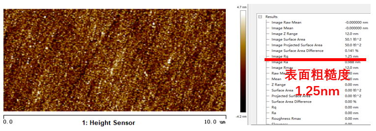
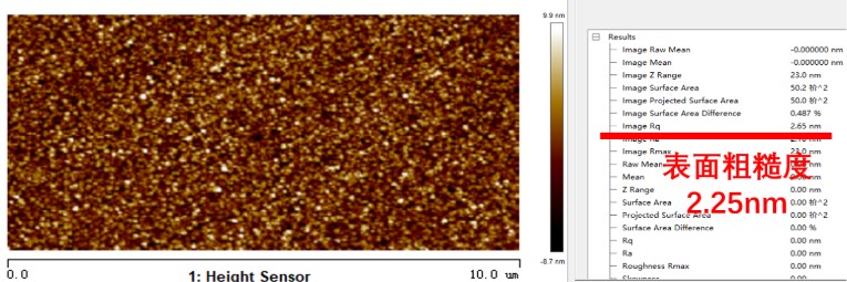
Figure 3 Surface roughness measurement after sputtering a 90 nm gold film on the quartz surface


Conclusion:The sputtering results of gold films with different thicknesses on double-sided polished quartz substrates demonstrate that the ion beam sputtering system hardly causes obvious variations in surface roughness in metal film deposition experiments with conventional thickness ranges.

Substrates with size below 4 inches and thickness less than 4 mm, with film uniformity limited to ±5% or better. Sputtering of magnetic materials is acceptable.
Samples: 4-inch specification.Minimum billing starts from 4 hours.Precious metal materials incur additional fees.Please refer to the operation manual for specific operating procedures.
The list below shows FAQs (click a question to view the answer). If your question is not listed, you can leave a message using the link.
FAQs
  • 01
    无法点火.没有辉光

    可能 氩气压力不够,添加氩气, 到0.12 MPa

Message Inquiry
If your question is not listed above, please email us at aemd@sjtu.edu.cn or click the button below to submit an inquiry.
Note: "@1" represents "@sjtu.edu.cn"
×