| Model: | ICP-SR |
|---|---|
| Function: | 1. Deep silicon etching using Bosch or non-Bosch processes; 2. TSV (Through-Silicon Via) deep silicon etching; 3. Surface silicon structure etching for SOI wafers. |
| Engineer: | Liu / +86-21- 34206126-6013 / minliu@1 |
| Location: | West Area – Thin Film II |
| Equipment ID: | WF2SDSE01 |

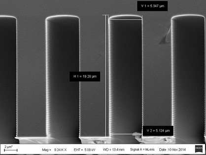
This system is primarily used for silicon and SOI micro/nanostructure etching. Typical applications include fabrication of nanoscale structures such as silicon waveguides and gratings, as well as deep silicon etching in MEMS devices.
Process / Testing Capabilities
Suitable for structures such as gratings and waveguides
Enables nanometer-scale control of etch depth
High etch rate for silicon
High selectivity to photoresist
High aspect ratio etching capability
Technical Specifications
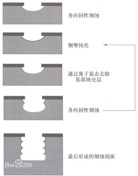
The etching step isotropically removes silicon
The passivation step deposits a protective polymer layer on sidewalls
Ion bombardment in the vertical direction removes the bottom passivation layer, enabling continued downward etching
This cyclic “etch–passivation–etch” mechanism suppresses lateral etching and ensures highly anisotropic, vertical profiles.
Address: 800 Dongchuan Road, Minhang District, Shanghai 200240, China
Tel: +86 21 3420 7734
Email: aemd@sjtu.edu.cn


