| Model: | ABM/6/500/DUV/DCCD/M |
|---|---|
| Function: | 1.Substrate: 6-inch and smaller silicon wafers, glass, etc.; 2.Lithography of micro-nano structures and device patterns with a minimum line width of 1 μm; 3.Single-sided alignment lithography. |
| Engineer: | Zhang / +86-21-34206126-6029 / captianzhangdi@1 |
| Location: | West Area – Lithography I |
| Equipment ID: | EODAMAL01 |

Including wafer lithography patterning, overlay alignment, thin film pattern fabrication, etc., supporting R&D and production in fields such as MEMS, semiconductors and optoelectronics.
Process/Testing Capabilities
Its working principle is to control the light intensity and time to expose the pattern on the photomask onto the spin-coated photosensitive material, and then realize the transfer of the pattern to the substrate after development.
Minimum feature size: 1 μm
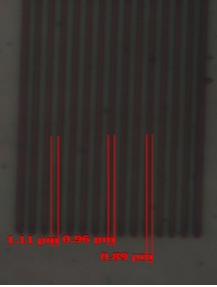
Semiconductor standard silicon wafers or glass wafers.
Sample size: 2", 3", 4".
Mask size: 5", 7"
For samples ≤ 6", dry solids, preheat for 10 minutes after turning on the light box power supply, and preheat for 10 minutes after turning on the mercury lamp. Please keep the machine clean and tidy after use.
The mercury lamp needs to be replaced.

Address: 800 Dongchuan Road, Minhang District, Shanghai 200240, China
Tel: +86 21 3420 7734
Email: aemd@sjtu.edu.cn