| Model: | EVG610 |
|---|---|
| Function: | 1.Double-sided photolithography patterning for wafers and fragments of 6 inches and below. 2.Minimum pattern resolution down to 0.8μm. 3.Provides high-precision alignment for bonded wafers and chips in conjunction with wafer bonding systems. 4.Can be matched with the EVG-510 bonder to realize wafer alignment and positioning functions. |
| Engineer: | Zhang / +86-21-34206126-6029 / captianzhangdi@1 |
| Location: | East Area – Lithography II (Canon) |
| Equipment ID: | ELT2DLS01 |

Including wafer lithography patterning, overlay alignment, thin film pattern fabrication, etc., supporting R&D and production in fields such as MEMS, semiconductors and optoelectronics.
Process/Testing Capabilities
Technical Specifications
Its working principle is to control the light intensity and time to expose the pattern on the photomask onto the spin-coated photosensitive material, and then realize the transfer of the pattern to the substrate after development.
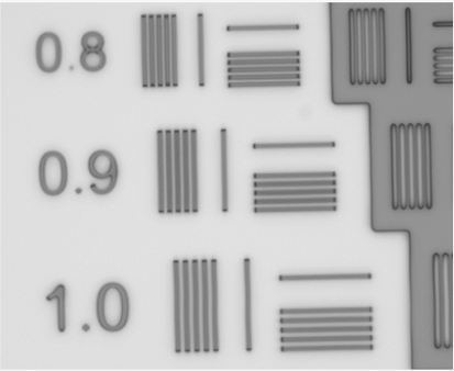
Minimum Line Width 0.8um
1.Samples shall be confirmed with the process engineer in advance.
2.Both the front and back sides of the sample shall be kept flat and clean.
3.Material fees are priced separately per piece.
4.For positive photoresist, the processing time is calculated at 1 wafer per 0.5 hours. Additional charges will apply for thickness exceeding 20μm.
5.For SU-8 photoresist with thickness exceeding 10μm, the processing time is calculated at 1 wafer per 1 hour.
Reinstall the mask or wafer.
Address: 800 Dongchuan Road, Minhang District, Shanghai 200240, China
Tel: +86 21 3420 7734
Email: aemd@sjtu.edu.cn


