Microwave Plasma Ashing Machine
Microwave Plasma Asher
Operating
Model: ION wave10
Function: 1.Photoresist ashing (stripping) after dry etching;2.Plasma modification on substrate surface;3. Substrate cleaning before photoresist coating to remove organic contaminants.
Engineer: Mr. Liu / +86-21- 34206126-6013 / minliu@1
Location: Thin Film Zone II, West Area
Equipment ID: WF2PASH01
  • Basic Equipment Information
  • Operating Principle
  • Typical Application Case
Main Application

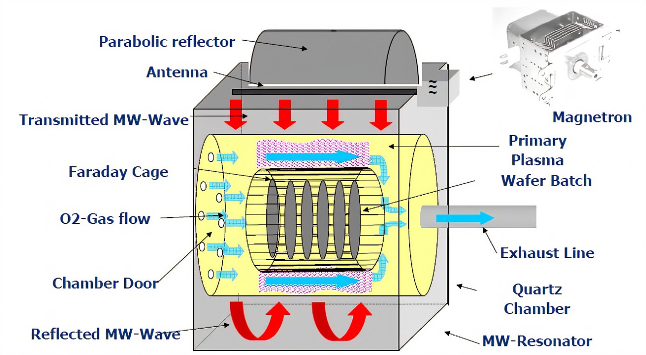
Microwave plasma photoresist stripper is mainly used for the chemical dry removal of various photoresists and substrate cleaning. Adopting a chemical etching working mode, it can achieve low damage to the substrate.


Process / Testing Capabilities

● Capable of removing various positive and negative photoresists;

● Able to eliminate a wide range of organic contaminants;

● Realize substrate surface modification, such as conversion between hydrophilicity and hydrophobicity;

● Photoresist removal rate: 0.2~0.4 μm/min;

● Etching mode: chemical etching.


Technical Specifications

  • Internal dimensions of reaction chamber: diameter 248 mm, depth 245 mm;
  • Compatible with 8-inch and smaller samples; process gases: N₂, O₂;
  • Maximum power: 600 W;
  • Microwave frequency: 2.45GHz;
  • Maximum batch capacity: 25 pieces of 6-inch wafers;
  • Chamber material: quartz.
In the quartz chamber, an appropriate amount of oxygen is introduced after vacuum pumping. Excited by the high-frequency electromagnetic field generated by the microwave power supply, oxygen is ionized into active plasma species including O2^-, O2^+, O^-, O^+, atomic oxygen and ozone. Assisted by the high-frequency electric field, these reactive species undergo oxidation reactions with photoresist and other organic materials on the substrate surface, producing highly volatile substances such as CO, CO2 and H2O. These gaseous by-products are exhausted by the vacuum pump to complete photoresist stripping. The corresponding principle is shown in the figure below.


This is a 6-inch silicon wafer coated with photoresist, which is marked with high-temperature adhesive tape for easy observation.

This is the silicon wafer after photoresist stripping, with the photoresist completely removed.

SU-8 photoresist and denatured photoresist cannot be removed. The removal of special photoresists requires prior confirmation.
The list below shows FAQs (click a question to view the answer). If your question is not listed, you can leave a message using the link.
FAQs
  • 01
    该设备是否可以去除SU8光刻胶?

    不行,该设备无法用于SU8胶的去除,只能去除普通正性和负性光刻胶。

Message Inquiry
If your question is not listed above, please email us at aemd@sjtu.edu.cn or click the button below to submit an inquiry.
Note: "@1" represents "@sjtu.edu.cn"
×