| Model: | Eitre 6 |
|---|---|
| Function: | Used for the fabrication of micro- and nano-scale patterned structures. Supports thermal nanoimprint, UV nanoimprint, and combined thermal and UV nanoimprint processes. |
| Engineer: | Xu / +86-21-34206126-6030 / lipingxu@1 |
| Location: | West Area – Lithography I |
| Equipment ID: | WPHNILE01 |

Enables the fabrication of micro- and nano-scale patterned structures. Supports thermal nanoimprint, UV nanoimprint, and simultaneous thermal and UV nanoimprint (STU™).
Incorporates a mature IPS soft template transfer process and technology. Compatible with templates made of nickel, silicon, and quartz, and applicable to a wide range of substrate materials, including Si, quartz, GaAs, and polymer films.
Achievable minimum feature size: ≤ 20 nm
Maximum imprint pressure: 80 bar
Applicable to the fabrication of nanophotonic crystals, subwavelength grating structures, solar cells, organic light-emitting diodes (OLEDs), and bio-microchannel structures.
Nanoimprint lithography transfers nanoscale patterns onto a resist-coated wafer through direct contact between the mold and the imprint resist. The resist is subsequently cured by UV exposure or thermal processing, followed by demolding.
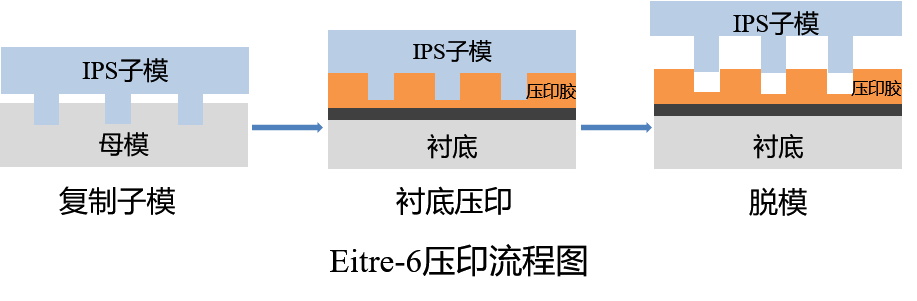
The Eitre-6 nanoimprint system utilizes gas-assisted soft imprint technology to ensure high uniformity and process consistency, while minimizing defect generation such as particle-induced damage.
Intermediate polymer stamp (IPS) transfer effectively protects the original master mold and extends its service lifetime.
The system configuration and imprint process flow are illustrated in the figure below.
Nanoimprint lithography can be applied to the fabrication of nanophotonic crystals, subwavelength grating structures, solar cells, organic light-emitting diodes(OLEDs),and bio-microchannel structures.
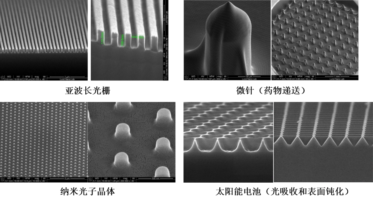
(All SEM images are sourced from nanoimprint results demonstrated by Obducat and are provided here as application examples of the nanoimprint system.)
1. The master mold must be treated with an anti-adhesion coating.
2. Wafer sample size: ≤ 6 inch; sample thickness: ≤ 2 mm.
3. The sample surface must be clean; particle contamination will severely affect imprint quality.
Anti-adhesion coatings can be applied using a Molecular Vapor Deposition (MVD) system.
Address: 800 Dongchuan Road, Minhang District, Shanghai 200240, China
Tel: +86 21 3420 7734
Email: aemd@sjtu.edu.cn


