| Model: | MPO100 |
|---|---|
| Function: | Structuring photoresist using two-photon polymerization (TPP) technology enables 3D lithography and 3D micro-printing of microstructures, with applications in optics, photonics, mechanics and biomedical engineering. |
| Engineer: | Xu / +86-21-34206126-6030 / lipingxu@1 |
| Location: | East Area – Lithography IIIA |
| Equipment ID: | ELT3MPO01 |

Equipped with a powerful 522 nm femtosecond laser source, it enables efficient and high-speed printing of SU8, AZ resist, ma-P100 resist, as well as metal layers and ORMOCER organic-inorganic hybrid resists. It can fabricate macroscopic structures with heights exceeding 1 millimeter, produce microstructures with exceptional surface quality and roughness as low as 10 nm, achieve a minimum feature size down to 100 nm, and deliver a scanning speed of over 1000 mm/s. The manufacturing processes for 3D nano-, micro- and macroscopic structures allow users to fully leverage various techniques for customized processing, and produce complex microstructures with high throughput in a single process step. It can be applied in fields such as micro-optics, optoelectronics, micromechanics, biomedical engineering, and quantum devices.
The MPO 100 is a two-photon polymerization (TPP) system for 3D lithography and 3D micro-printing, which uses two-photon polymerization technology to structure photoresist or metallic materials. This system features high-precision 3D lithography and high-throughput 3D micro-printing, supporting high-resolution additive and subtractive manufacturing. Additive manufacturing involves precise layer-by-layer construction, while subtractive manufacturing removes materials with high precision to fabricate complex functional microstructures.
It can be used in fields such as micro-optics, optoelectronics, micromechanics, biomedical engineering, and quantum devices:
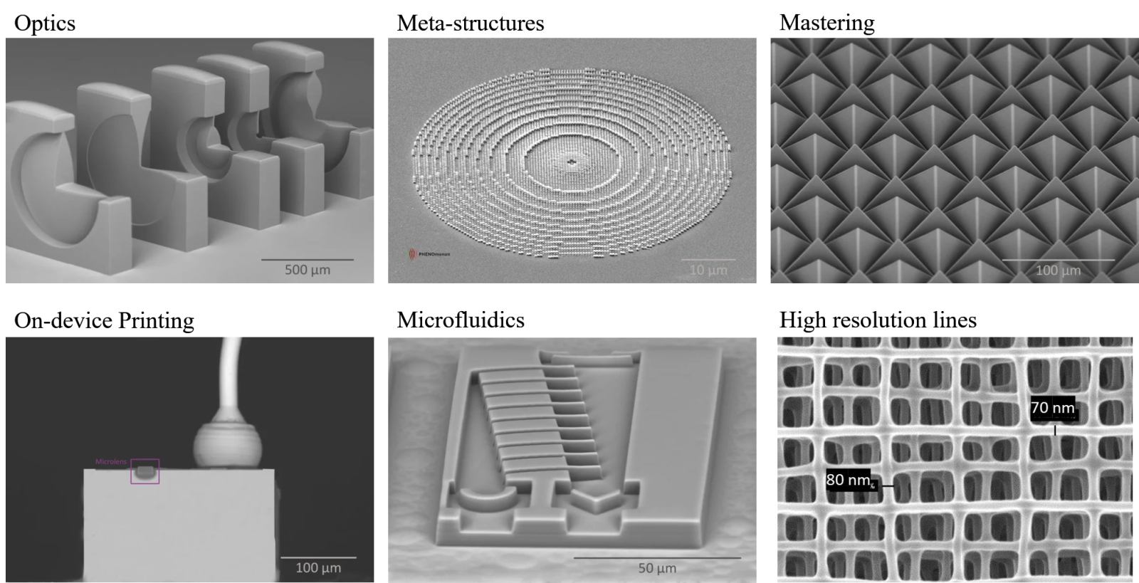
(All the above SEM photos are from the 3D microlithography achievement exhibition of Heidelberg Company, serving as application examples for this 3D microlithography equipment)
1.1.Substrate size ≤ 4 inches, thickness ≤ 4 cm.
2.When the characteristic dimension of the sample is ≤ 500 nm, the substrate must be treated with O₂ plasma to enhance adhesion.
3.Users shall prepare layout files by themselves. Supported layout file formats: 3D structures: .obj, .stl; grayscale exposure: .bmp, .tif, .png.
Software such as Solidworks and Blender can be used for layout drawing.

Address: 800 Dongchuan Road, Minhang District, Shanghai 200240, China
Tel: +86 21 3420 7734
Email: aemd@sjtu.edu.cn