| Model: | Auriga |
|---|---|
| Function: | Fabrication of two-dimensional and three-dimensional structures through patterning deposition, cutting, and etching of samples at the micro-nano scale |
| Engineer: | Wang / +86-21-34207734-8006 / wangying@1 |
| Location: | West Area – Thin Film IA |
| Equipment ID: | WF1ZFIB01 |

In a dual-beam system, the field emission scanning electron microscope is mainly used to observe and analyze the microscopic morphology of materials, while the focused ion beam is employed to perform operations on samples at the micro-nano scale, such as pattern deposition, cutting, etching, transmission sample preparation, circuit repair, and atom probe tip fabrication.
1. Pt, W, C, SiO₂, XeF₂ gas injection system: Capable of controlled deposition as well as enhanced or selective etching induced by ion beams and electron beams.
2. Oxford nanomanipulator (including electrical property testing): Transmission electron microscope sampling system that can extract tiny samples after FIB cutting, and cooperate with FIB to transport and manipulate nanomaterials.
3. 3D imaging system: Enables automatic cutting, automatic imaging of samples, and 3D reconstruction after superimposing all images.
4. Micro-nano processing system: A hardware and software system equipped with ion beam deposition and capable of processing complex patterns.
5. Equipped with an electron beam gun, enabling non-interference processing or etching of insulating materials.
6. Maximum sample size no larger than 150 mm; ultimate vacuum: better than 5×10⁻⁷ Torr.
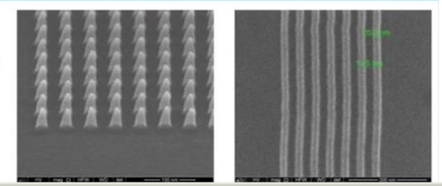
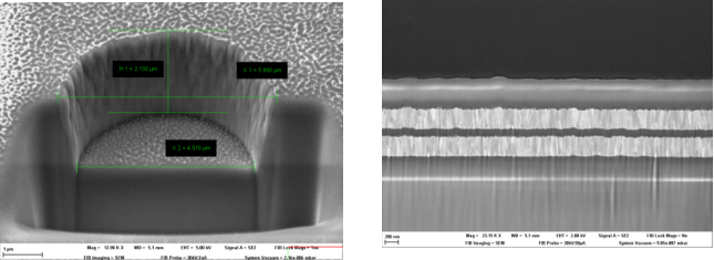
Focused Ion Beam (FIB) technology is based on the core principle of the synergistic effect of electric and magnetic fields, which enables the ion beam to be focused down to the sub-micrometer or even nanometer scale. By precisely controlling the deflection and acceleration systems to regulate the scanning path of the ion beam, accurate analysis and mask-free processing of micro-nano scale patterns can be achieved. This technology is a method for processing materials at the micro-nano scale using a high-intensity focused ion beam. FIB technology allows precise cutting of samples and reveals their morphology and dimensional characteristics by observing their cross-sections. In addition, this technology can be combined with elemental analysis techniques such as EDS to analyze surface and cross-sectional compositions. Meanwhile, FIB technology also features multiple functions including material lift-off, deposition, ion implantation, and material modification.
Deposition and etching
Cross-section observation
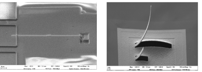
Circuit repair and 3D processing
Magnetic and powder samples are prohibited. Samples must be kept clean, and direct contact with hands is forbidden. The size should preferably not exceed 2×2 cm.
A focused ion beam (FIB) is used to perform micro-cutting on the sample surface, with a cutting thickness of approximately 2 nanometers. Simultaneously, a scanning electron microscope (SEM) is employed to image the sample. By repeatedly performing the aforementioned cutting and imaging steps combined with computer image processing technology, the three-dimensional spatial structural information of the sample is obtained.
Using an ion beam to bombard the sample surface, or combining it with organic gases to perform effective selective etching of the sample (circuit cutting), deposition of metals or dielectric materials (new circuit connection).
Samples are operated under an electron beam or ion beam, and their morphology must be clearly observed; otherwise, precise sample preparation cannot be achieved.
A. The sample processing position should be close to the edge.
B. Whether the sample is conductive or not; specimens with poor conductivity shall be subjected to gold sputtering treatment.

Address: 800 Dongchuan Road, Minhang District, Shanghai 200240, China
Tel: +86 21 3420 7734
Email: aemd@sjtu.edu.cn