Plasma Surface Treatment / Cleaning Machine
HARRICK Plasma Cleaner
Operating
Model: PDC002
Function: 1. Plasma cleaning of substrate surface 2. Surface modification treatment of substrate (O₂ or N₂)
Engineer: Mr.Fu / +86-21- 34206126-6010 / xuecheng.f@1
Location: Thin Film Zone IA, West Area
Equipment ID: WF1HPCL01
  • Basic Equipment Information
  • Operating Principle
  • Typical Application Case
Main Application

Remove residual photoresist from incomplete development before evaporation or etching, so as to ensure the adhesion of evaporated metal layers and enable smoother etching processes. It can also modify the substrate before spin-coating to achieve more uniform photoresist coating.


Process / Testing Capabilities

Three power levels are optional, with the power ranges as follows:

● Low power level: 716 V DC voltage, 10 mA DC current, operating power of 7.16 W, compliant with requirements.

● Medium power level: 720 V DC voltage, 15 mA DC current, operating power of 10.15 W, compliant with requirements.

● High power level: 740 V DC voltage, 40 mA DC current, operating power of 29.6 W.


Technical Specifications
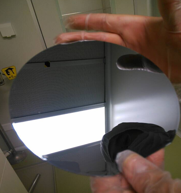
  • Cleaning chamber dimensions: length 6.5 inches (165 mm), diameter 6 inches (152 mm), with an openable chamber cover.
  • Suitable for surface treatment of 6-inch silicon wafers; the maximum residual photoresist removal rate is 4 nm/min.
The working principle of the plasma cleaner is mainly based on the physical and chemical effects of plasma. In a vacuum chamber, a radio frequency power supply generates high-energy plasma carrying positive and negative charges, which forms electric and magnetic fields. The plasma collides with the material surface to bombard and strip off contaminants for cleaning. Meanwhile, plasma reacts chemically with the surface to produce volatile by-products, achieving further removal of contaminants.
Low power enables rapid and efficient substrate surface treatment, while effectively protecting the base material. The figure shows the hydrophilicity and hydrophobicity comparison of silicon wafers before and after modification.

Before modification

After modification

Samples larger than 6 inches are not acceptable.Cleaning and stripping of thick photoresist are not supported.
It generates glow discharge ionizing radiation and requires standardized operation.
The list below shows FAQs (click a question to view the answer). If your question is not listed, you can leave a message using the link.
FAQs
  • 01
    开机后迟迟不见辉光

    检查腔门是否关闭严紧,可能会有松动

Message Inquiry
If your question is not listed above, please email us at aemd@sjtu.edu.cn or click the button below to submit an inquiry.
Note: "@1" represents "@sjtu.edu.cn"
×