| Model: | 3030EX6 |
|---|---|
| Function: | 180nm semiconductor process node lithography process |
| Engineer: | Xu / +86-21-34206126-6018 / xu.jian@1 |
| Location: | East Area – Lithography II (Canon) |
| Equipment ID: | ELT2DUV01 |

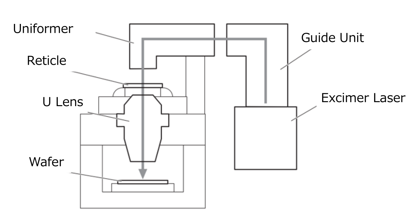
It is used to transfer the chip circuit patterns on the photomask to the silicon wafer, serving as a core step in IC manufacturing. The basic working principle of a photolithography machine is to project patterns onto the silicon wafer by utilizing optical principles. It mainly consists of a light source, convex lenses, photoresist, a control system, and other components. This equipment is mainly used to achieve fully automatic alignment lithography at the 0.18 μm semiconductor process technology node.
Optical path structure diagram
This device adopts a 248 nm excimer laser as the light source, raising the minimum process node to the 180 nm level. It employs step-and-repeat projection lithography for the exposure process. The light source passes through a reticle, and after adjustment by optical lenses and compensation for various imaging errors, the circuit information on the reticle is projected onto the wafer in the form of reduced imaging. Meanwhile, a high-precision stage carries the silicon wafer in a step-and-repeat manner to achieve continuous exposure die by die until the entire wafer is covered with reticle patterns. The equipment features high precision and extremely fast exposure speed, and the entire exposure process is fully automated without manual intervention.
Carry out fully automatic gluing, exposure and development for 8-inch, 6-inch, 4-inch and 3-inch specifications respectively in different time periods according to demand.
Currently using UV135g with a thickness of 400nm.
Address: 800 Dongchuan Road, Minhang District, Shanghai 200240, China
Tel: +86 21 3420 7734
Email: aemd@sjtu.edu.cn


