| Model: | DSE200s |
|---|---|
| Function: | 1.Deep silicon etching using Bosch or non-Bosch processes; 2.TSV (Through-Silicon Via) deep silicon etching; 3.Surface silicon structure etching for SOI wafers. |
| Engineer: | Liu / +86-21- 34206126-6013 / minliu@1 |
| Location: | West Area – Thin Film II |
| Equipment ID: | WF2NDSE02 |

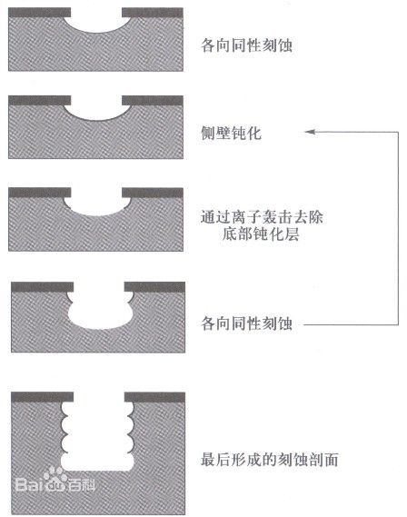
This system is primarily used for deep silicon etching and supports both Bosch and non-Bosch processes, enabling broad process coverage.
It is equipped with advanced fast-response hardware and optimized software control specifically designed for Bosch cyclic processing. Combined with advanced process technologies, the system delivers excellent performance for high-aspect-ratio etching, meeting a wide range of process requirements.
Process / Testing Capabilities
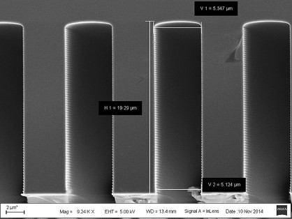
Maximum etch rate: ~6 μm/min. Selectivity to photoresist: up to 50:1. Aspect ratio: >30:1. Sidewall roughness: <50 nm.
Technical Specifications
Designed for 6-inch wafers; compatible with 4-inch, 3-inch wafers and irregular samples. Supports diced samples (with carrier wafer mounting). Applicable to glass substrates such as SOG (Spin-On Glass).
This method, originally proposed by Robert Bosch, enables deep silicon etching with high aspect ratios and well-defined vertical structures.
Address: 800 Dongchuan Road, Minhang District, Shanghai 200240, China
Tel: +86 21 3420 7734
Email: aemd@sjtu.edu.cn


