| Model: | Plsmalab100 |
|---|---|
| Function: | Low-temperature (300 ℃) deposition of thin films such as silicon oxide, silicon nitride, amorphous silicon, silicon oxynitride and silicon carbide. |
| Engineer: | Liu / +86-21- 34206126-6013 / minliu@1 |
| Location: | West Area – Thin Film II |
| Equipment ID: | WF2OCVD01 |

Radio frequency is used to ionize gases containing thin-film constituent atoms to locally generate plasma, which promotes a series of gas-phase chemical reactions and forms solid thin films on the sample surface. It is mainly applied to the low-temperature growth of films such as SiOx, SiNx and a-Si.
Process/Testing Capability
Technical Specifications
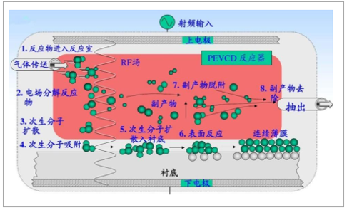
PECVD technology operates under low air pressure. It utilizes low-temperature plasma to generate glow discharge on the cathode of the process chamber, namely the tray where samples are placed. The sample is heated to a preset temperature by glow discharge or an additional heating element, followed by the introduction of an appropriate amount of process gases. These gases undergo a series of chemical and plasma reactions, ultimately forming a solid thin film on the sample surface. The schematic diagram of its process principle is shown in the figure.

Address: 800 Dongchuan Road, Minhang District, Shanghai 200240, China
Tel: +86 21 3420 7734
Email: aemd@sjtu.edu.cn