| Model: | RPX-540 |
|---|---|
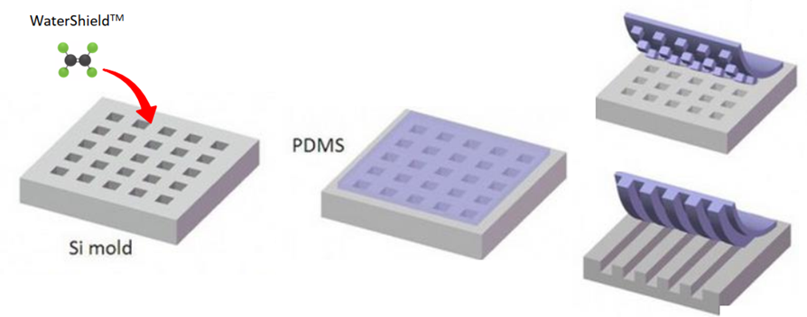
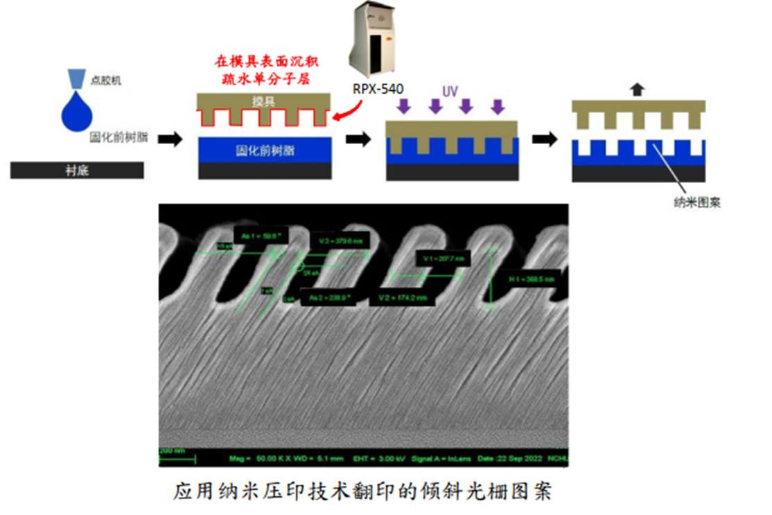
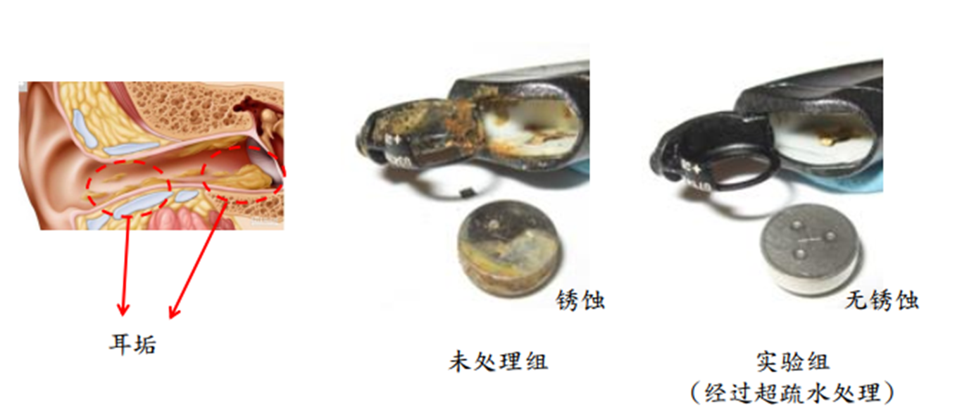
| Function: | 1. This equipment can perform surface modification and functionalization on high-aspect-ratio structures of semiconductor-compatible and biocompatible substrates such as silicon wafers and glass slides in a vapor-phase environment. It can form highly uniform monolayer thin films to achieve hydrophobic surfaces, hydrophilic surfaces, and functional surfaces with specific functional groups, supporting relevant semiconductor and biochemical experiments; 2. This device can be used in conjunction with the nanoimprint lithography system purchased in the second phase of the AEMD platform. It effectively improves the surface release quality of nanoimprinting and further enhances the pattern fabrication capability of the nanoimprint equipment; 3. As a fully functional surface modification system, this instrument supports multiple deposition modes, including ALD (Atomic Layer Deposition), CVD (Chemical Vapor Deposition) and SAM (Self-Assembled Monolayer) deposition. |
| Engineer: | Wu / +86-21- 34206126-6028 / lynn_wu@1 |
| Location: | East Area – Thin Film IV |
| Equipment ID: | EFM4MVD01 |

1. It enables surface modification of high-aspect-ratio structures on semiconductor-compatible and biocompatible substrates such as silicon wafers and glass slides in a vapor phase environment, to fabricate highly uniform monolayer thin films with hydrophobic, hydrophilic, and specific functional group-modified surfaces.
2. As a full-function surface modification system, it supports multiple deposition methods including ALD (Atomic Layer Deposition), CVD (Chemical Vapor Deposition) and SAM (Self-Assembled Monolayer) deposition.
Process/Testing Capability
Technical Specifications

Address: 800 Dongchuan Road, Minhang District, Shanghai 200240, China
Tel: +86 21 3420 7734
Email: aemd@sjtu.edu.cn