| Model: | DWL66+ |
|---|---|
| Function: | 600nm~Micron-level process capability photoresist direct writing function, overlay direct writing function and 3D grayscale lithography function |
| Engineer: | Wang / +86-21-34206126-6005 / fdwang@1 |
| Location: | East Area – Lithography IIIA |
| Equipment ID: | ELT3DWL01 |

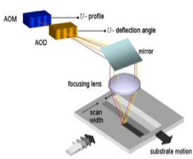
As a maskless lithography technology, laser direct writing lithography uses a laser beam with variable intensity to perform variable-dose exposure on the photoresist material on the surface of a substrate. After development, the required patterns are formed on the surface of the photoresist layer. It enables high-precision processing without the need for fabricating masks, and is applicable to the processing of various materials, including glass, metals, silicon wafers, semiconductors, polymers, and others.
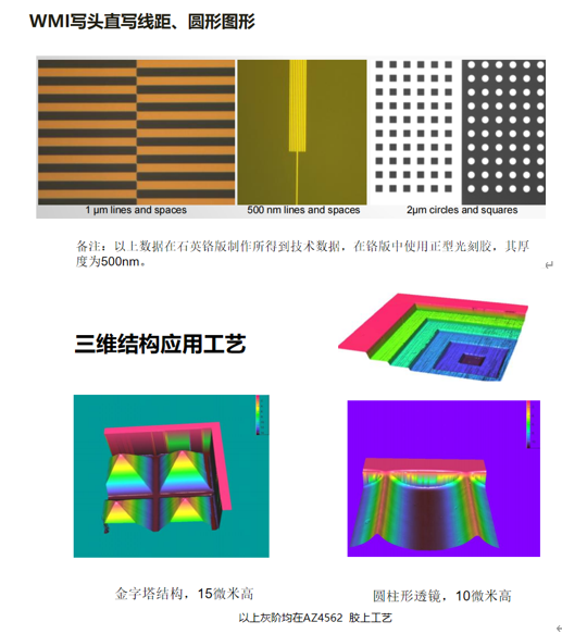
It can be applied to the processing of a variety of different materials, including glass, metal, silicon wafers, semiconductors, polymers, etc. It is widely used in fields such as microelectronics, biomedicine, optics and nanodevices, and can be used to fabricate microprocessors, sensors, microstructures, biochips, microfluidic chips, MEMS and other microelectronic devices.
1.The maximum sample size shall not exceed nine inches.
2.The minimum sample size is 1.5cm*1.5cm. Samples that are too small will cause difficulties in automatic focusing and are prone to colliding with the writing head during patterning!
3.Ensure that the exposed pattern is at least 0.5cm away from the edge of the sample.
4.Special attention for circular samples: Ensure that each patterning position is at least 0.5cm away from the nearest edge of the sample.
5.For exposed pattern arrays: Be sure to keep the outer periphery of the array at least 0.5cm away from the edge of the sample.
Please initialize the stage.

Address: 800 Dongchuan Road, Minhang District, Shanghai 200240, China
Tel: +86 21 3420 7734
Email: aemd@sjtu.edu.cn