| Model: | ACT8 |
|---|---|
| Function: | Fully automatic coating and developing for 180 nm semiconductor process node. |
| Engineer: | Xu / +86-21-34206126-6052 / hui.xu25951@1 |
| Location: | East Area – Lithography II (Canon) |
| Equipment ID: | ELT2ACT01 |

Supports HMDS hydrophobic modification, photoresist spin coating, soft bake, PEB (post-exposure bake), puddle static developing, post bake, etc. for 4/6/8-inch standard semiconductor wafers. Supports fully automatic coating, exposure, and developing processes for 6/8-inch wafers with Canon DUV Stepper.
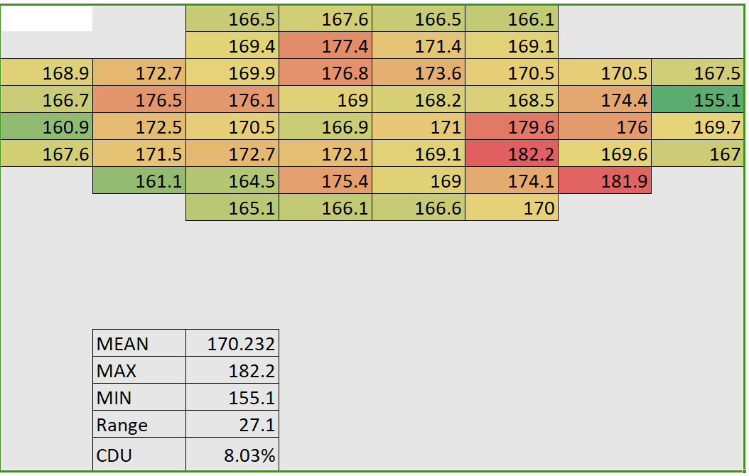
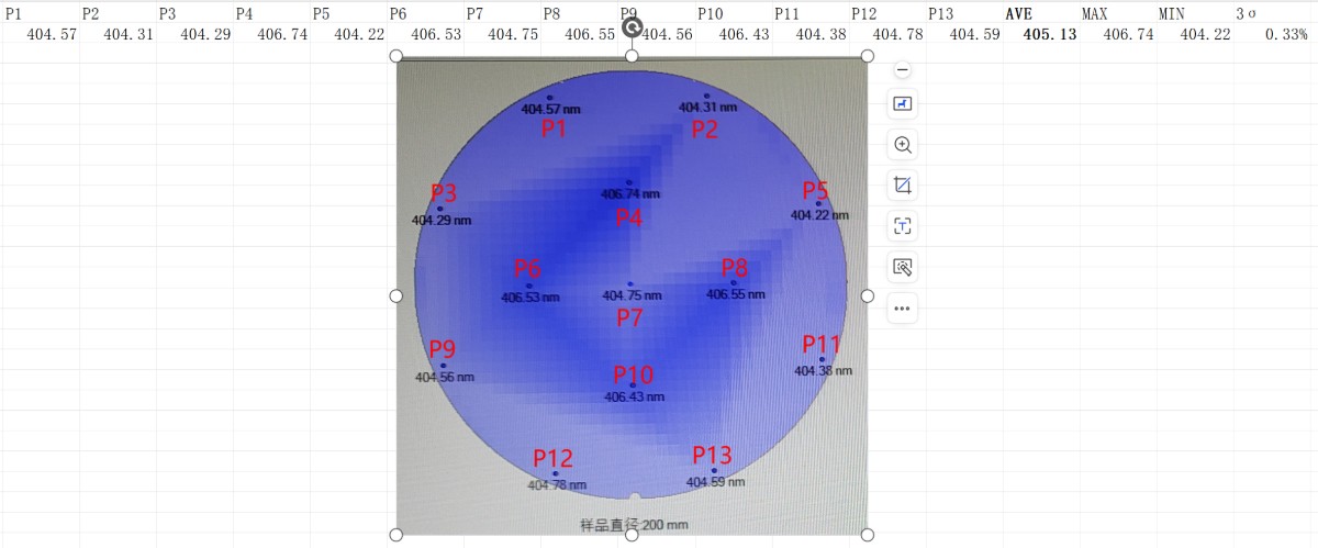
Film thickness uniformity accuracy ≤1%; within-wafer CD uniformity after developing (CDU) 3σ ≤10%; hot plate temperature range: 50°C ~ 350°C.
1. Pre-coating hydrophobic modification using HMDS (hexamethyldisilazane).
2. Photoresist spin coating and edge bead removal; adjustable film thickness and controllable edge bead removal width.
3. Soft bake / PEB / hard bake; multiple hot plate options, temperature range 50°C ~ 350°C, high accuracy.
4. Developing using static puddle process; SH nozzle and LD nozzle provide high flow rate with low impact. After developing, DIW and high-speed spin rinsing are used to dry the wafer surface.
5. High-speed chill plate cooling: wafer temperature can be lowered to 23°C within 60 seconds.
6. Fully automatic processing; the above functions can be combined according to process requirements, or each function can be used individually.
7. HMDS – coating – soft bake – cooling: 7 min/wafer.
8. PEB – cooling – developing – hard bake – cooling: 8 min/wafer.
8-inch standard semiconductor wafers (for 4/6-inch wafers, please contact the relevant engineer).
Switching between different wafer sizes requires 2 weeks. Please check the website or AEMD platform announcements for current equipment status.
The resist pump only supports low-viscosity photoresists; thick resists are not supported.
No.
No. Only supports 4/6-inch flat wafers and 8-inch notch wafers.
Address: 800 Dongchuan Road, Minhang District, Shanghai 200240, China
Tel: +86 21 3420 7734
Email: aemd@sjtu.edu.cn


