为科研工作提供
服务的大型仪器设备共享平台
服务的大型仪器设备共享平台


鼠标向下滚动

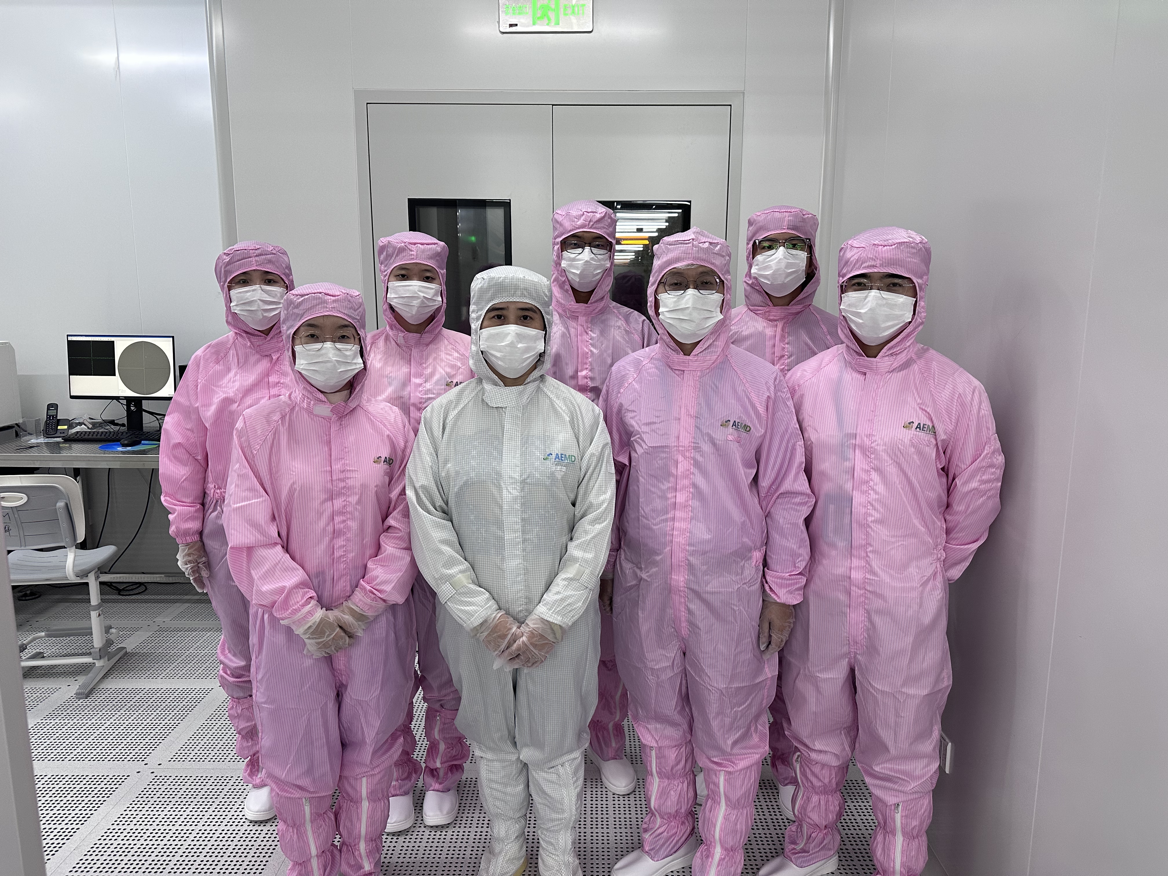
2025年12月31日下午,AEMD平台在先进电子材料与器件平台东区会议室组织举办了2025年度集体生日会,平台全体教职工齐聚一堂,共同庆祝这一温馨而有意义的时刻。

AEMD平台祝您元旦快乐,幸福安康!
为进一步提升平台开放共享水平,展示先进实验条件,增进校内外用户对AEMD平台科研能力的了解与认知,2024年10月20日至11月16日,AEMD平台连续三周举办了三场“走进AEMD平台二三期”参观活动,吸引了来自校内多个学院的教师与学生,以及校外合作单位的科研用户参与。
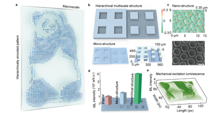
近日,上海交通大学集成电路学院(信息与电子工程学院)微米纳米加工技术全国重点实验室臧法珩副教授团队在柔性力学发光与可视化传感领域取得新进展。
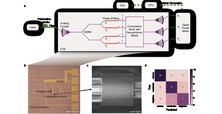
近期,上海交通大学集成电路学院(信息与电子工程学院)郭旭涵教授、苏翼凯教授课题组与上海理工大学顾敏院士课题组在SOI(Silicon on Insulator, 绝缘衬底上的硅)平台上成功实现了基于散射介质的机器学习任务推理。
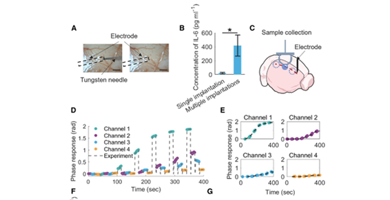
近日,上海交通大学生物医学工程学院医疗机器人研究院邱广宇、杨广中团队在脑机接口术中急性炎症反应动态检测领域取得进展,相关成果以“Intraoperative and Spatiotemporal Mapping of Acute Inflammation Response During Neuroelectrode Implantation”(脑机接口神经电极植入术中脑区急性炎症反应的时空动态检测)为题在国际著名期刊《Matter》上发表。

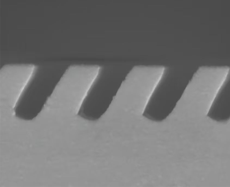
研究采用原子层沉积(ALD)工艺在硅衬底上生长了35 nm以下不同厚度的超薄氮化铝(AlN)晶态薄膜。利用椭圆偏振光谱法在275 nm~900 nm波长范围内测量并拟合薄膜的厚度及折射率、消光系数等光学参数。利用原子力显微镜(AFM)表征AlN晶粒尺寸随生长循环数的变化,并计算得到薄膜表面粗糙度用于辅助椭偏模型拟合。针对ALD工艺特点建立合适的椭偏模型,可获得AlN超薄膜的生长速率为0.535 Å/cycle,ALN超薄膜的折射率随着生长循环数的增加而增大并逐渐趋于稳定,薄膜厚度为6.88 nm时其折射率为1.6535,薄膜厚度为33.01 nm时其折射率为1.8731。该模型为超薄介质薄膜提供了稳定、可靠的椭偏法表征。
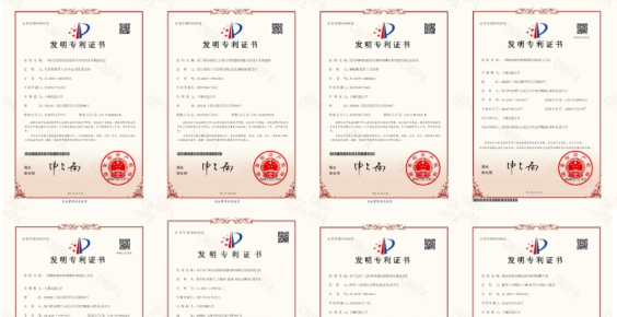
AEMD平台充分发挥交大人“求真务实、努力拼搏、敢为人先、与日俱进”的精神,不断产出国内外基础性、前瞻性、特色性的原创成果,努力建设成为能够实现重大突破的开放性科研平台,为加快实现我国高水平科技自立自强贡献更大的力量。平台员工累积申请及授权发明专利14余项,先后应邀在微纳制造领域会议发表大会主题报告及特邀报告20余次,在微纳加工领域的基础研究及应用开发方面取得了突出的研究成果,受到了国内外同行的广泛关注,AEMD平台已初步发展成为该领域具有领先优势的关键元器件制造技术研究与开发的平台。

根据AEMD平台的数据,自成立以来,已经支撑用户发表了超过300篇学术论文,申请了多项专利,有力推动了微纳加工技术的学术与产业进步。